PCB Design Guideline
- 14.08.2019
- admin

Good Quality Production Data
Whether
is prototyping or mass production, it is important to create quality
data for production to reduce rejection rates. While CAD is able to
inspect the board through Design Rule Check, data
that has been designed indiscriminately can affect the yield of the
production.
The design practices that are useful
for both prototype and mass manufacturing for “quality stability” in
production..
- 1. Put radius at the board corner
- 2. Breakaway board
- 3. Machining guide hole
- 4. Reference hole / sub-reference hole
- 5. Fiducial Marks
- 6. Part number / model name
1 Radius at the corner
Radius of about 5.0mm at the board corner
Adding radius at the board corner has the following advantages.
- Prevents injuries during handling of the board due to sharp edges
- Prevents damage to other boards and objects during the manufacturing processes
- Prevents component loss due to sharp edges is easier to trapped in the transfer line during assembly
- Prevents chipping and damage to packaging materials due to impact and vibration during transportation
Radius of 5.0mm is recommended. Smaller radius may not prevent the above phenomenons. Consider adding radius at the corners of both breakaway board and the main boards.
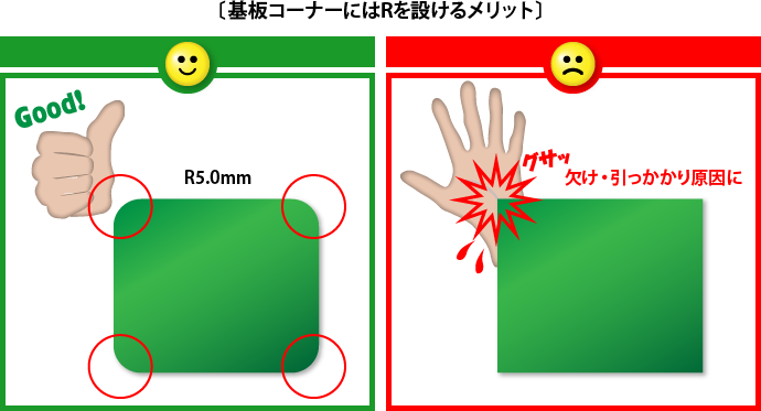

- Radius at the main board and breakaway board.
- Set radius as large as possible. Recommended is 5.0mm
2 Breakaway board
The benefits of adding a breakaway boards
- Prevent boards from being damaged during manufacturing, packaging and shipping processes
- Make it easier to support mounter mounting
- Machining guide holes, mounting recognition marks, reference holes, sub-reference holes, and radius corner can be placed at the breakaway board.
Breakaway
boards are not only useful for positioning and mounting, but also
useful in protecting the main board. It is recommended to design the
breakaway board in the longitudinal direction of the board related to
the mounting of the board to the transfer line..
Though it may increase the board area
and costs, it will be insignificant if the yield and quality of the
board can be control consistently during production.it is a very
effective way to stabilize quality. Please consider adding a discarded
board.
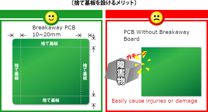
- The width of the discarded board is usually around 10.0 to 20.0 mm.
- It is a good idea to add solid copper foil that is divided into discarded substrates to prevent warping and expansion / contraction.
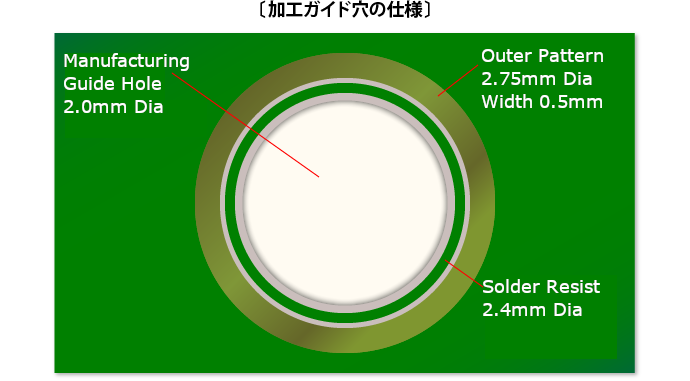
3 Machining guide hole
Recommended
Size and Positions
- Size: φ2.05mm (NTH) or φ1.55mm (NTH)
- Placement position:
- 2x
Holes on the board around the edge
- 1x for
preventing reverse loading
- Holes
should be placed asymmetrical to prevent wrong orientation
- Approximately 5.0mm from the board edge
- Extra holes maybe required to hold on to the main boards during cutting process enabling the routing process to remove the breakaway PCB.
4 Reference hole / sub-reference hole
Reference hole / sub-reference hole to be used in the mounting process.
Recommended Size and Positions
Hole diameter: φ4.0mm (NTH)
Sub-reference hole: φ4.0x5.0mm (LNTH)
Placed horizontally
with respect to mounting flow directions
Advantages.
- This is the reference hole for mounting the board to the mounter.
- Fix the board and prevent mounting displacement
- Used as a “reference hole for positioning” when inserting lead parts using an automatic insertion machine
The
secondary reference hole is an ellipse in consideration of dimensional
shrinkage of the board. There
are SMD component mounters that do not require a “reference hole /
sub-reference hole”, but there are many mounter devices that use
positioning reference pins and transfer pins in the mounter. 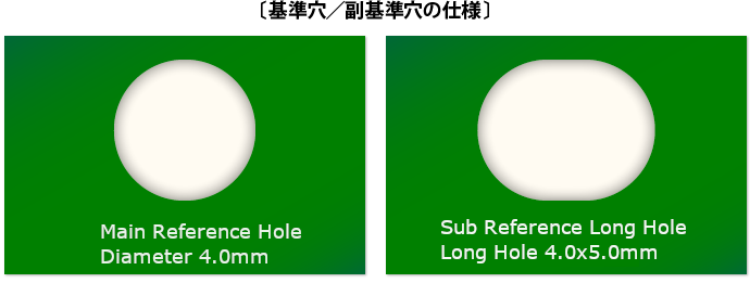
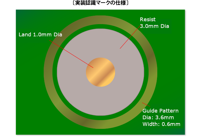
5 Fiducial Mark
Fiducial mark is used to align the board with the auto insertion machine.
Recommended Size and Positionsattern size:
Pattern Diameter φ1.0 mm
Resist opening size: φ3.0 mm
Guard pattern: Ring with outer diameter of φ3.9 mm, inner diameter of
φ3.3 mm
Positions: 2 on the PCB, 1 for preventing reverse loading 3 or more
for location
Placed in asymmetrical position
For
narrow pitch parts with a pitch of less than 0.5 mm or parts with leads
under the package, such as BGA, fiducial mark is added to the
individual part to improve the mounting accuracy.
The
placement position should be asymmetric to prevent incorrect mounting
on the front and back surfaces, so that they do not overlap even if
they are turned over or rotated 180 degrees. Component mounting errors are
prevented.
In order to prevent the mounting recognition mark from disappearing by etching at the time of pattern formation (the process of dissolving unnecessary portions of copper foil by the corrosive action of chemicals), a solid pattern should be placed around for protection purposes.
- Required
for auto placement and auto insert machine
- Placing a fiducial mark on each each side of the board increases accuracy.
6 Part number / Model name
For Identification
Easy to recognize board
Reduce mistakes with similar boards
Additional information such as Serial Number, Revision Number, Lot Number would be useful for identification.

- Printed
in legible and in prominent locations
Tags: PCB Design Guideline, PCB Design Good Practice